
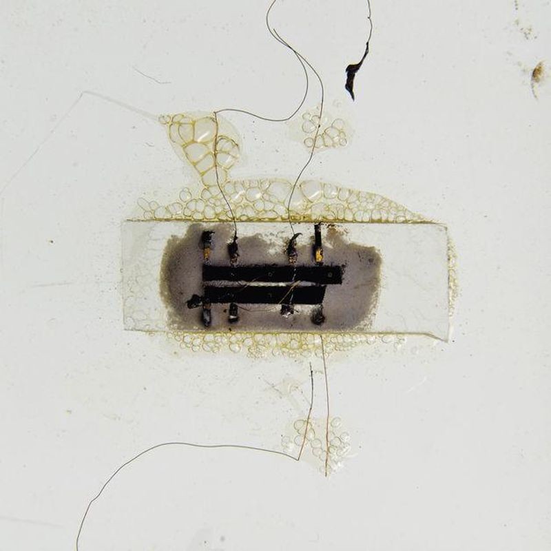
Kilby Phase Shift Oscillator Circuit (1958). Photo: Christie’s Auction House
Christie’s auction sale notice (May 22, 2014) of the only known phase-shift oscillator circuit built by Nobel Prize winner Jack Kilby in private hands proclaimed him as the inventor “of the integrated circuit on a single chip.” While he played an important role in the development of the IC, Kilby’s 1958 prototype was but one of many attempts to build such a device that had been underway for several years. In his Nobel Prize acceptance speech he acknowledged “the contributions of thousands of engineers and scientists in laboratories and production facilities all over the world.” This article describes some of those contributors, several of whose approaches were earlier and more fully integrated.
Integrated circuits comprise the basic building blocks of today’s electronic systems. Also known as a computer chip or microchip, an IC is an analog and/or digital circuit together with internal connections deposited on a single piece of semiconducting material. Jack Morton, head of transistor manufacturing at Bell Telephone Laboratories, described an early conception of such a circuit. In a 1949 internal report he noted: “Imagine a technique in which…the connecting leads and passive elements are ‘printed’ in one continuous fabrication process. …We do not know the technology of doing these things… Here then is the challenge.”
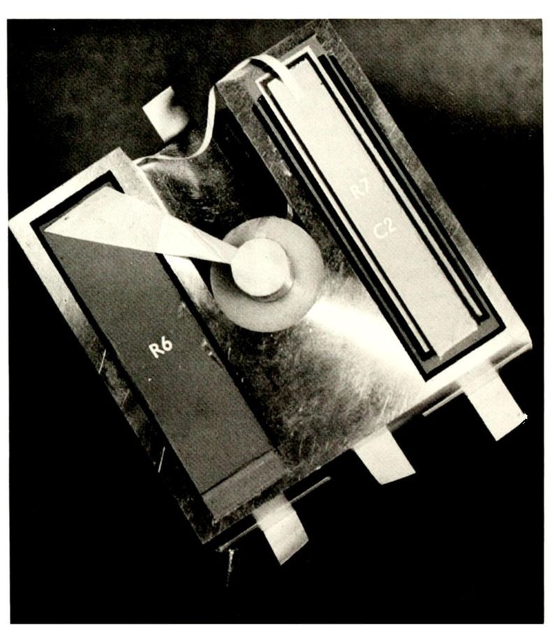
Conceptual model of Dummer’s integrated amplifier (1957). Photo: Telecommunications Research Establishment
1952, G. W. A. Dummer, a manager at the Telecommunications Research Establishment, in Malvern, England suggested that technology had advanced to the point that: “With the advent of the transistor and the work in semiconductors generally, it seems now possible to envisage electronic equipment in a solid block with no connecting wires.” Although Dummer’s own efforts took nearly a decade to bear fruit [1], other researchers did succeed in producing working devices in the years before 1958.
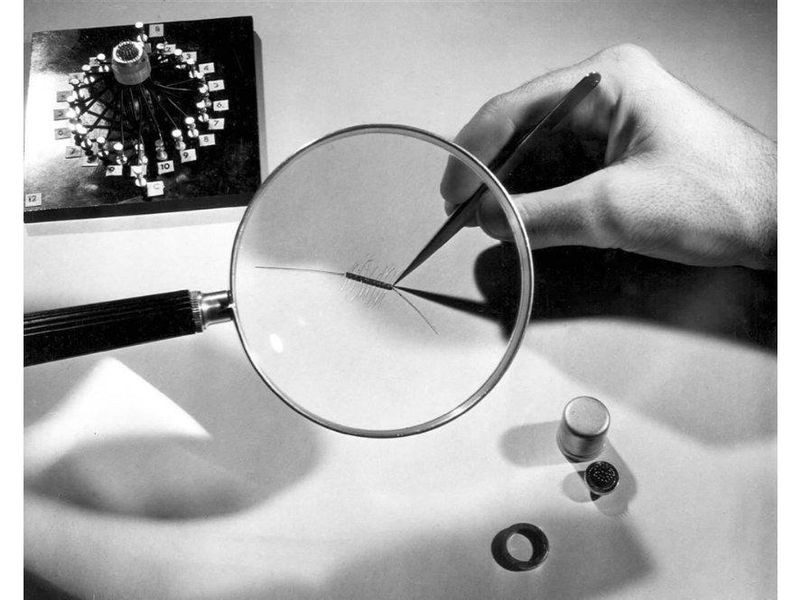
RCA integrated semiconductor shift register (1957). Photo: RCA Corporation
Within a few years of the transistor’s invention, scientists across the globe pursued the idea of manufacturing multiple devices on a single chip. Using the original Bell Labs’ point-contact structure, Werner Jacobi at Siemens, Germany filed a patent for a single-chip, five-transistor amplifier in 1949. Sidney Darlington of Bell Telephone Laboratories patented circuits with two and three junction transistors in 1953. And in 1957 Yasuro Tarui fabricated a “quadrapole” transistor, a form of unipolar (field-effect transistor) and a bipolar junction transistor on the same chip, at MITI’s Electrotechnical Laboratory near Tokyo. [2] All these devices featured designs where several transistors could share a common active area with no electrical isolation to separate them from each other.
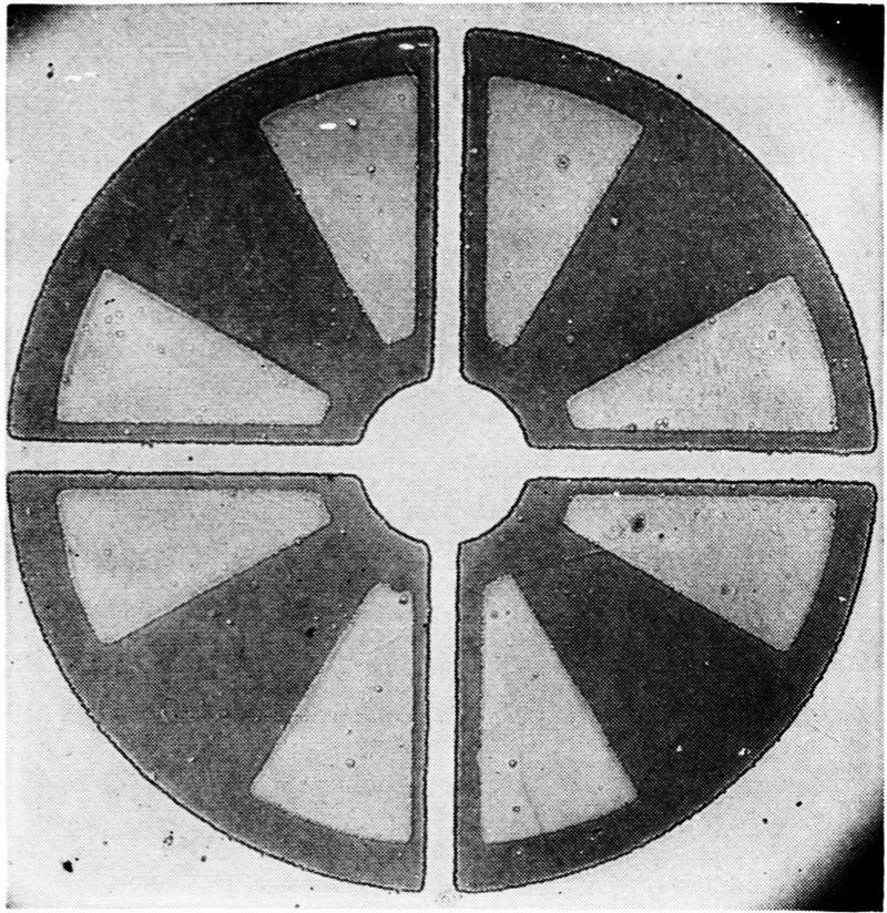
Bell Labs “stepping transistor” four-stage ring counter (1955). Photo: Bell Telephone Laboratories
Certain complex counting and switching circuits formed a class of special purpose integrated functions that could also be accomplished without requiring electrical isolation between the active devices. Using a network of RC (resistor-capacitor) elements on a single germanium chip, Harwick Johnson designed a complete phase shift oscillator circuit in 1953 at RCA in New Jersey. While his device did not yield a commercial product, his interest in integrating complete electronic functions continued when he supervised Torkel Wallmark’s work on a shift register for the Air Force. Under the title “Integrated Semiconductor Devices” an article in the RCA Laboratories annual report for 1957 included a photograph of Wallmark’s “integrated device which combines in one unit the functions to be performed by a whole assembly of capacitors, resistors, amplifiers and switches.” [3]
At IBM, Poughkeepsie, NY in 1954, Joseph Logue supervised Rick Dill’s design of an integrated ring-counter using “double-base diodes.” Dill succeeded in building a single silicon chip with four stable states, essentially a four-bit ring counter. The same year saw the launch of an effort to create a similar counter at Bell Labs. Led by Ian Ross, who would later become President of Bell Labs, H. H. Loar and L. A. D’Asaro fabricated a “stepping transistor”, a four-stage ring counter that replaced 8 transistors, & dozens of diodes, resistors & capacitors with a single silicon chip, in 1955. [4]
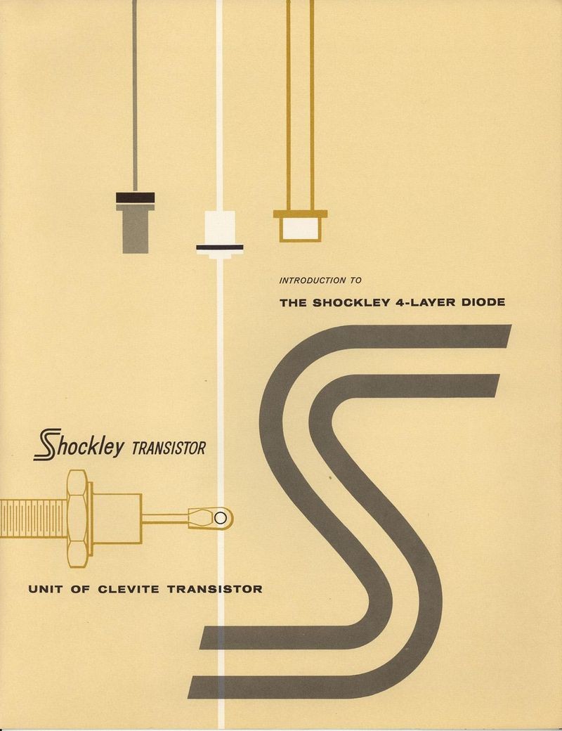
Shockley 4-Layer Diode Brochure Cover. Photo: Clevite Corporation
Both the Bell and IBM counters were based on a four-layer diode structure originally conceived by William Shockley who realized that a PNPN device offered two stable operating conditions. As a switch that could remain in one of two states, he saw it as a solid-state replacement for mechanical crosspoint switches in the Bell Telephone system. Equivalent to a circuit comprising two transistors, a diode, and two resistors, Shockley’s obsession with implementing this integrated function at his own start-up company in Mountain View, California, led to the 1957 departure of eight key scientists, who then founded Fairchild Semiconductor. Although Shockley eventually moved the device into pilot production, it was rendered obsolete by more general purpose IC functions produced by his ex-employees at their new company.
Texas Instruments, Dallas hired Jack Kilby to manage the company’s program of circuit miniaturization for aerospace applications. Previous approaches, such as PNPN devices, had produced truly integrated devices but offered only a limited set of useful circuit functions. Kilby realized that if he could manufacture each circuit component as a unique physical element within the semiconductor material, designers could then connect them into any desired configuration. [5]
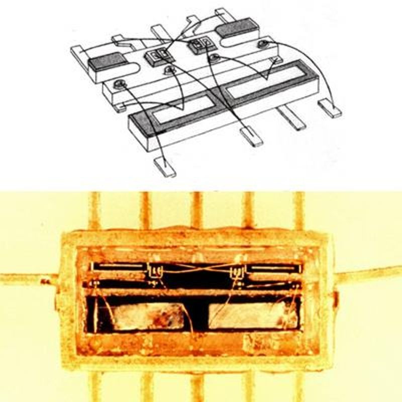
Type 502 Bistable Multivibrator Solid Circuit (1960). Photo: Texas Instruments
On September 12, 1958, Kilby demonstrated his phase-shift oscillator prototype built with germanium transistor chips containing distinct transistor, capacitor, and resistor components. Aided by technicians Pat Harbrecht and Tom Yeargan, he connected the separate elements into an oscillator circuit using fine gold wires. One week later they produced an amplifier. T.I. announced Kilby’s Solid Circuit Semiconductor Network concept in March 1959 and introduced its first commercial device, the Type 502 Silicon Bistable Multivibrator, one year later.
Although several components could be formed on a single bar of material, TI’s approach required careful handcrafting of each unit. Electrical isolation between components involved etching “weird shapes” in the surrounding material [6] and making connections between them required attaching wires, called flying-wires, above the surface of the chip. This was not a practical production technique and only a few dozen solid circuits were ever shipped to customers for evaluation.
Beginning in 1957, Westinghouse Electric pursued research that led to a contract to develop “molecular” electronic devices for the U. S. Air Force. Based on the ideas of MIT professor Arthur von Hippel, this concept emerged many years later in the form of nanotechnology but in the near term led to a series of integrated analog circuits known as Functional Electronic Blocks (FEBs). In 1959, John D. Husher at the Youngwood, PA facility cut grooves across the surface of power transistor chips to create islands of discrete component elements that he connected with flying wires into FEBs such as audio amplifiers, detectors, and filters. [6]
When Jack Kilby began to pursue his idea in July 1958, the founders of Fairchild Semiconductor, Palo Alto, CA were focused on building their first transistors. Even so, in that same month Robert Noyce took time out to document on page 46 of his patent notebook an idea for interconnecting multiple diodes on a single wafer to fabricate an integrated function table. [7] However, as with as the Bell Labs and other approaches, he described a specialized structure that could not be easily adapted for general-purpose designs.
Fairchild co-founder Jean Hoerni’s application of the masking and insulating properties of silicon dioxide to implement the planar manufacturing process for transistors revived Noyce’s interest in circuit integration early in 1959. Under the title “Methods of isolating multiple devices,” on January 23 he wrote on page 70 of his notebook: “In many applications now it would be desirable to make multiple devices on a single piece of silicon in order to be able to make interconnections between the devices as part of the manufacturing process.” He noted that the technique could be applied “to transistors as well as diodes ... (to build) a generalized logic element” and included a schematic for an adder circuit.
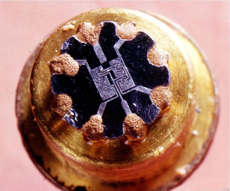
Fairchild Semiconductor Type “F” flip-flop (1960). Photo: Fritz Goro/Time & Life Pictures/Getty Images
Jay Last, another Fairchild co-founder, assembled a team of engineers to translate Noyce’s ideas into working devices. They produced the first planar integrated circuit, a 4 transistor, 5 resistor flip-flop in May 1960. [8] Under the trade name µLogic (Micrologic), the company announced the type “F” flip-flop function to the public in March 1961. Five additional circuits, including the type “G” gate function that served in NASA’s Apollo Guidance Computer, were introduced in October.
All major semiconductor manufacturers licensed resulting Fairchild patents and converted their circuit design activities to the planar process that continues to underlie the billion transistor chips of today.
Fairchild and TI engaged in litigation over the patents for many years. The courts eventually ruled in Noyce’s favor but by then the companies had settled on a commercial resolution. Kilby and Noyce both received the National Medal of Science in 1979 and today are celebrated as co-inventors of the integrated circuit. But as Noyce noted in an IEEE oral history “There is no doubt in my mind that if that invention had not arisen at Fairchild that it would have arisen elsewhere in the very near future. It was an idea whose time had come and the technology had developed to a point where it was viable.” [9]
While the Kilby prototype offered at Christie’s may not have been the first integrated circuit, it is possibly the most valuable. The owners withdrew the lot from the auction when bidding reached “only” $800,000. They were seeking at least $1,000,000.
This article is based on papers contributed to special issues of the IEEE Annals of the History of Computing devoted to “The Early History of Microcircuitry” published as Volume 34, Number 1 and Volume 35, Number 1 in January 2012 and 2013 respectively. References to these papers and other resources are listed below.